30. Stress-Strain Behavior of a Cu Nanowire
The stress-strain behavior of a Cu nanowire can be readily simulated with the MedeA Environment using the embedded atom method (EAM) and MedeA Deformation. In this illustration a monocrystalline nanowire is stretched in the [100] direction. The simulations show an initial elastic region with a linear increase in stress, which reaches a maximum just before the onset of slip in (111) planes. Upon further strain, the model forms additional slip planes and necking until its break point is reached.
Keywords: Nanowire, stress-strain, necking, slip, fracture, EAM, deformation
30.1. Purpose
This application note illustrates the ability of the MedeA Environment, particularly the MedeA Deformation module combined with LAMMPS [1] to simulate the deformation of metals under strain and to compute the stress-strain behavior of such systems. A monocrystalline nanowire of Cu with a diameter of 3.3 nm oriented in the [100] direction of this face-centered cubic material is employed as a specific example.
30.2. Model Construction
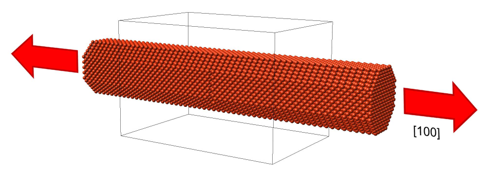
Starting from the unit cell of elemental Cu, which is readily retrieved from the databases available within the MedeA Environment, a model of a nanowire can be conveniently constructed using an integrated suite of building tools. To initiate a desired break point, atoms near the middle of the slab are deleted, thereby creating a nano-notch. The resulting model is shown in Figure 30.2.1.

Figure 30.2.1 Model of a Cu nanowire containing 10,189 atoms oriented along the [100] direction of this cubic material. The direction of strain is indicated by the red arrows. An atomic-scale notch near the middle of the model is used to initiate the separation.
Using the MedeA EAM library of potentials for the embedded atom method (EAM), the form of Adams et al. [2] is selected and parameters are assigned to the model atoms. These simple steps create a model with assigned forcefield parameters for use in MedeA LAMMPS based molecular dynamics simulations.
30.3. Stress-Strain Calculation
The properties of the nanowire model can now be explored. For example, the cell dimension in the main wire axis direction can be set to a series of values. For each value, the cell is stretched using the structure from the previous step, and a short molecular dynamics simulation carried out (in this illustration the temperature employed was 150 K and the dynamics run for 10 ps) and the last structure of each dynamics simulation was relaxed by energy minimization. The MedeA Deformation capabilities of the MedeA Environment with extensive loop construction, analysis, and reporting capabilities, facilitate the construction of such computational workflows.
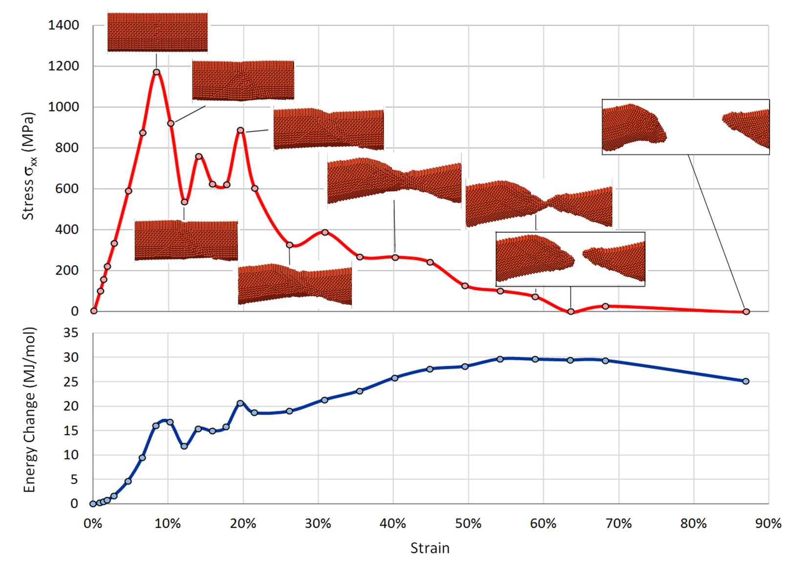
Figure 30.3.1 displays the result of such a simulation. As expected, near equilibrium the total energy of the system depends quadratically on the strain and the stress increases linearly in this harmonic regime. When slip occurs, the stress of the system decreases in an oscillatory manner, which is also seen in the total energy of the system. As more slip planes develop and their displacements increase, the wire forms a neck, which becomes thinner upon further stretching until the breakpoint is reached. At this point the stress drops to zero. Due to the blunting of the tips of the model, the total energy decreases after separation.
Using this model and in this simulation, the maximum stress is 1170 MPa. This refers to a monocrystalline nanowire with a cross section of 11.2 nm2 in a box, which has a cross section of 52.3 nm2. Since the computed stress refers to the box, one obtains a maximum stress of 5464 MPa for the wire itself. This is, of course, much higher than values reported for polycrystalline copper, namely 220 MPa for the ultimate tensile strength. Furthermore, the present simulations are performed at a temperature of 150 K where one expects a stiff behavior. However, nanoscale systems have interesting and unique properties and bulk like behavior for such systems should not be expected, as discussed below.

Figure 30.3.1 Stress-strain behavior of a Cu nanowire computed with an embedded atom potential using MedeA Deformation and MedeA LAMMPS. After each step straining the material, the system is subject to a short molecular dynamics run followed by an energy minimization. Note the harmonic behavior up to the point of highest stress, where slip in the (111) planes sets in. The tip blunting after fracture leads to a small lowering of the total energy of the system. The stress refers to a simulation box with a cross section of 52.27 nm2; the cross section of the nanowire itself is 11.16 nm2.
30.4. Significance
The MedeA Environment makes the exploration of system variables straightforward. For example, in the present case, the dimensions of the wire, the crystallographic orientation, and the size and location of the notch can be varied, the temperature and duration of the simulation explored, and the effect of alloy composition on stress strain behavior investigated. Grain boundaries can be built into the initial model and their effect on the stress-strain curve could be investigated. The MedeA Environment and MedeA Deformation in particular make such systematic analyses straightforward. In the present case for example, the nanoscale impact of dopant species at different concentrations can be explored making use of the forcefield by Zhou et al. [3] which facilitates the simulation of Cu and 15 common metallic alloying elements. The insights obtained by such simulations can be invaluable in analyzing and targeting experimental investigation. Analogous simulations can also be performed for brittle ionic materials using Buckingham-type potentials, which are also available within the MedeA Environment. Given sufficient computational resources, such simulations may also be performed using the quantum mechanical VASP program to compute energies, forces, and stress tensors. MedeA VASP can be invoked as one of the stages within the MedeA Environment.
An exciting new possibility has become available through machine learned potentials (MLPs) and their facile generation in the MedeA environment, using the MedeA MLP and MedeA MLPG modules. Using this technology, the simulation of the mechanical response of diverse systems, including partially oxidized metals, to stress and strain, as demonstrated in the present example is made readily accessible and does not rely on the existence of suitable generic forcefields.
The present example is an illustration of the capabilities of MedeA Deformation and MedeA LAMMPS rather than a detailed investigation of the stress-strain behavior of metallic nanowires. However, it is worth noting that such studies have been reported. For example, Liang et al. [4] investigated the role of surface effects on the elastic behavior of Cu nanowires, describing interesting insights into the origin of nanoscale properties, and providing the basis for focused materials optimization.
MedeA modules used in this application
- MedeA Environment
- MedeA Deformation
- MedeA LAMMPS
- MedeA EAM
| [1] | S. Plimpton, “Fast Parallel Algorithms for Short-Range Molecular Dynamics”, J. Comp. Phys. 117, 1 (1995) link |
| [2] | J. B. Adams et al., “Self-diffusion and impurity diffusion of fcc metals using the five-frequency model and the Embedded Atom Method”, J. Mater. Res. 4,102-112 (1989) link |
| [3] | X. W. Zhou et al., “Misfit-energy-increasing dislocations in vapor-deposited CoFe/NiFe multilayers”, Phys. Rev. B 69, 144113 (2004) link |
| [4] | H. Liang et al., “Size-dependent elasticity of nanowires: Nonlinear effects”, Phys. Rev. B 71, 241403 (2005) link |
| download: | pdf |
|---|