MedeA Electronics
At-a-Glance
MedeA®[1] Electronics computes key electronic properties of metals, semiconductors, and insulators including isoenergy (Fermi) surfaces, electronic contributions to the electrical and thermal conductivity, thermoelectric power, and effective masses.
Key Benefits
- Straightforward setup of the calculation and automated distribution over a large number of tasks
- Easy selection of isosurface energy and isosurface sheets for display
- Transport quantities displayed as a function of temperature, chemical-potential shift (rigid-band doping), or carrier density
- Adaptation of fundamental band gap for refined calculation of transport properties
Due to the Pauli principle, only the electronic states at the Fermi energy, and within a narrow energy range of width kBT around it, govern a material’s response to external electric or magnetic fields, or temperature gradients. For this reason, insight into the energy distribution of these states and the nature of their wave functions is of utmost importance for understanding the material’s properties.
MedeA Electronics explores the electronic states within a narrow energy range about the Fermi energy by giving access to ground-state properties, such as Fermi surfaces, specific heats, and effective masses as well as transport properties, like the electronic contributions to the electrical and thermal conductivities and the thermoelectric power.
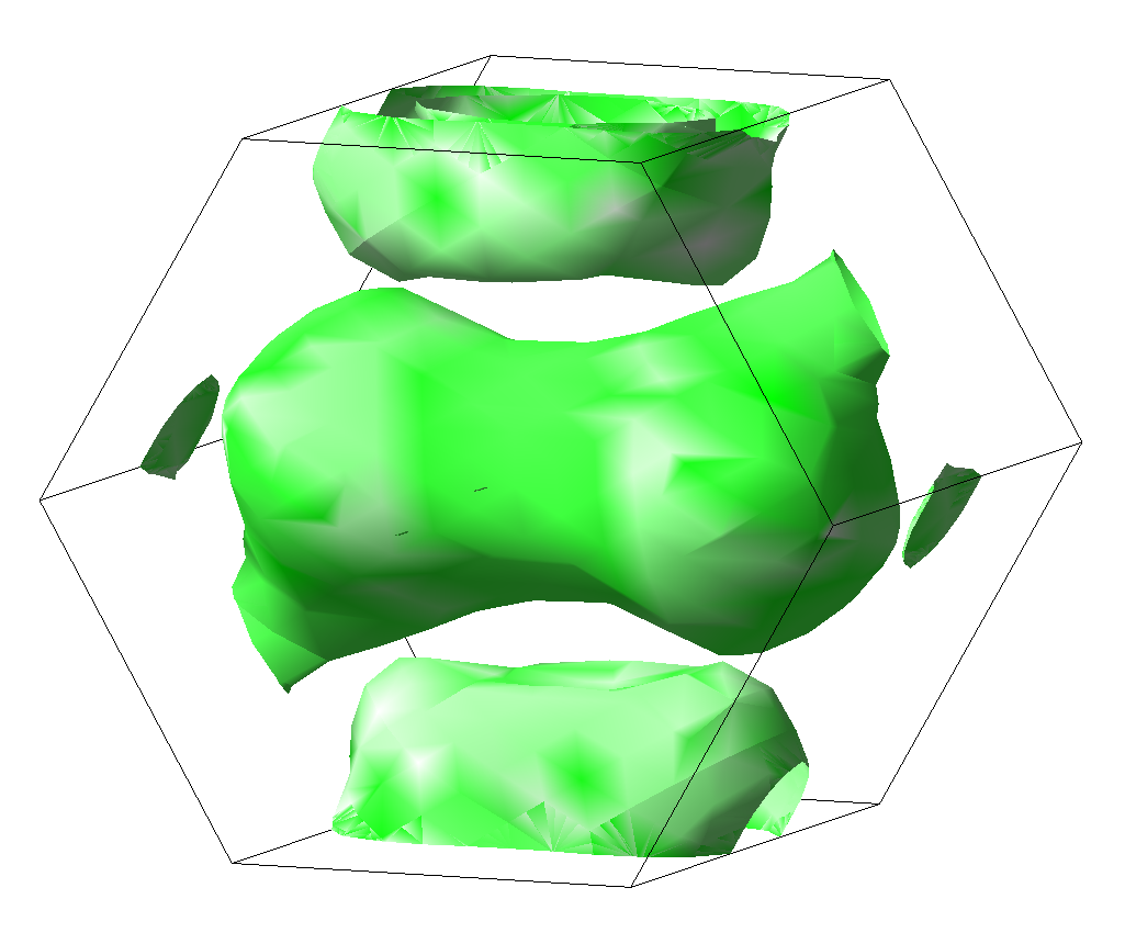
For example, the Fermi surface of MoO2, as shown in the Figure below, identifies three different sheets, namely, an electron-like peanut-shaped Fermi surface centered at the \(\Gamma\) point and two smaller hole-like Fermi surfaces each centered at the Y point, explaining the anisotropic electrical conductivity. Both angle-resolved photoemission spectroscopy and de Haas-van Alphen measurements show very good agreement with calculated Fermi surfaces, and thus underline the predictive power of first-principles calculations [2].

Fermi surface of molybdenum dioxide calculated using MedeA Electronics
The concept of effective masses has gained importance in describing the response of electrons (and holes) to external electric and magnetic fields. Effective masses are determined by the curvature of the bands near the Fermi energy in metals or the bands close to the valence band maximum and conduction band minimum in semiconductors. Given the electronic states in that energy region effective masses can thus be straightforwardly calculated. As an example, calculated effective masses of silicon’s hole and electron states are given in the following table and found in almost perfect agreement with experimental data.
| Exp. [3] | Exp. [4] | MedeA | |
|---|---|---|---|
| Electrons | |||
| Long Eff. Mass | 0.92 | 0.98 | 0.94 |
| Trans Eff. Mass | 0.19 | 0.19 | 0.20 |
| DOS Mass | 1.06 | 1.08 | 1.09 |
| Conductivity Mass | 0.26 | 0.27 | |
| Heavy Hole | |||
| Eff. Mass | 0.54 | 0.49 | 0.67 |
| Light Hole | |||
| Eff. Mass | 0.15 | 0.16 | 0.13 |
| Split-off Band | |||
| Eff. Mass | 0.23 | 0.24 | 0.22 |
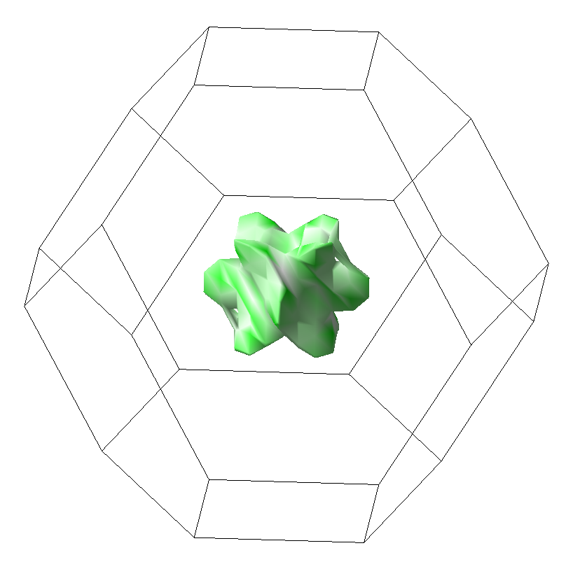
Deviations are observed for the heavy-hole mass, which are related to the strong anisotropy of the \(\Gamma\)-point hole states as nicely demonstrated in the figure below illustrating the isosurface of the electronic states of Si at 0.7 eV below the valence band maximum.

Isoenergy surface of Si at -0.7 eV calculated using MedeA Electronics
Key Features
- Automated setup, execution, and processing of background jobs through an intuitive user interface to calculate properties
- Full integration in the MedeA Environment takes advantage of MedeA’s robust JobServer and TaskServer Infrastructure
- Efficient management of calculations across the desired number of CPU cores
- Electronic eigenvalues computed with MedeA VASP
- Automatic detection and use of space-group symmetry
Properties
- Three-dimensional isosurfaces of electronic energies (Fermi surfaces) in k-space
- Interactive analysis of effective masses for each band at any point in k-space
- Interpolated electronic band structure displayed for orientation
- Highly accurate effective mass tensors for selected electron or hole bands at requested points in k-space
- Electrical conductivity, thermal conductivity
- Thermoelectric power (Seebeck coefficient)
- Electronic specific heat
- Pauli paramagnetic susceptibility
- Hall coefficient
Value of Integration
Required Modules
- MedeA Environment
- MedeA VASP
Find Out More
Learn more about MedeA Electronics by checking out the following on Materials Design Application Notes page:
- Thermoelectric Properties of Bi2Te3 as calculated using MedeA Electronics.
Check out the Datasheets on MedeA Fermi Surface and MedeA Electronic Transport for additional information.
| [1] | MedeA and Materials Design are registered trademarks of Materials Design, Inc. |
| [2] | J. Moosburger-Will, J. Kündel, M. Klemm, S. Horn, P. Hofmann, U. Schwingenschlögl, and V. Eyert, Phys. Rev. B 79, 115113 (2009) (DOI) |
| [3] | H. D.. Barber, Solid State Electronics 10, 1039 (1967) (DOI) |
| [4] | https://www.ioffe.ru/SVA/NSM/Semicond/Si/bandstr.html |
| download: | pdf |
|---|